
Automated X-Ray Inspection
In recent years, automated X-Ray inspection (AXI) has grown as a new type technology. Similar to an optical inspection, an x-ray inspection produces images of the object. The image is then processed by image processing software that detects the position and size/ shape of expected features (for process optimization) or presence/ absence of unexpected/ unintended objects or features (for anomaly detection). Instead of visible light it uses x-rays (typically generated by an x-ray tube) that pass through the object. Opposite the x-ray emitter is a detector that either converts x-ray into visible light (creating an optical image which is then picked up by a camera) or sensor arrays that directly pick up the x-ray and convert it into an electronic image. The image is produced due to the different absorption of x-rays when passing through the object and can therefore reveal structures inside the object that are hidden from outside view.
AXI, automated X-ray inspection systems are able to monitor a variety of aspects of a printed circuit board assembly production. It can not only check the solder joints that are under packages such as BGAs, CSPs and flip chips where the solder joints are hidden but also reveal many defects in solder joints that may not be visible with ordinary optical inspection equipment. They would normally be placed after the solder process to monitor defects in PCBs after leaving the soldering process.
As one significant improvement in AXI, automated X-ray inspection, not only are 2D techniques available, but machines utilizing 3D technology are available and give significant improvements in performance. For 3D AXI equipment, PCBWay uses model Xscan-7130,it has high-efficiency Inspection system also it has secured the best stability and safety in the industry (amount of surface leakage less than 1μsv/h).
In order to know the inspection coverage of AXI clearer, the table below as reference.
X-ray Inspection
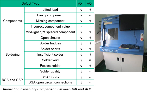
Due to the development of Surface Mount Technology and increasing complexities of electronic products, high-density and small PCBs account for the majority. As a main form of structural test and inspection, Automated Optical Inspection is only applicable for defects that are relatively easier found such as open circuits, solder bridges, solder shorts, insufficient solder and excess solder. However, because pins of BGAs are hidden under the chip package, it’s difficult to test them only based on light. That’s why Automated X-ray Inspection (AXI) is required.
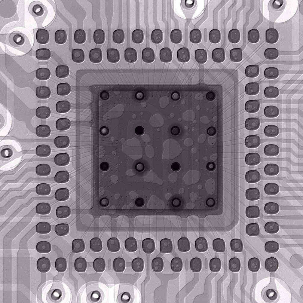
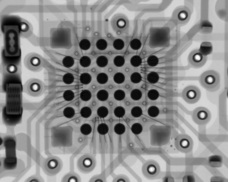
Belonging to the same structural test and inspection category, AXI shares the same principle with AOI, that is, inspection is carried out through capturing images. The difference between them lies in the source in that AOI depends on light source to capture images while AXI on X-ray. Materials absorb X rays according to their atomic weight proportion. Materials made of heavy elements get more X rays absorbed while those made of light elements get fewer. As a result, materials absorbing more X rays are displayed more obvious or darker in their images than those absorbing fewer rays. When it comes to PCBA, solder joints are made of materials with heavy elements while other parts such as most packages, silicon ICs and component leads are made of materials with light elements. Therefore, high-quality solder joints should look darker or more obvious on images than other parts.
Based on its working principles and capabilities, AXI is applied to test circuit boards containing components with array-style packaging or fine pitch packaging including BGAs, CGAs (Column Grid Arrays), CSPs (Chip Size Package), etc. AXI is usually placed in the assembly process, just after the last soldering no matter wave soldering or reflow soldering. Furthermore, AXI is usually applied coupled with boundary scan test, ICT and functional test in order to obtain optimal inspection results.
AXI features some advantages as a type of structural test and inspection:
• Some defects can be found in the early stage of printed circuit board assembly process;
• It is contributive to the cost reduction of defects;
• It stops defects from flooding among remaining PCB assembly or even clients’ practical projects.
AXI equipment is classified into two categories: 2D and 3D equipment. For 2D AXI equipment, GoJGo uses model VIEWX2000, responsible for inspecting PCBA manufacturing defects including opens, shorts, insufficient solder, excessive solder, missing electrical parts, misaligned components, solder voiding etc.
Although AXI and AOI have the same working principles and play similar roles in PCB assembly production line, defects they can detect differ to some extent. The following table shows comparison between AXI and AOI in terms of their inspection coverage.
Free PCB Request for Quotation (RFQ)
1. You can send email to us (tedchen163@yahoo.com). We will provide you with a
solution to make your PCB cost lower.
2. GoJGo receive your order,review the first,if there are questions,we will communicate with you
the first time and answer you about the lead time.
3. Our Engineering department will review this order with relevant departments,Produced in the best
process and in the shortest time.
4. Before shipment,we will talk with you about the shipping time and shipping method.
If you would like to customize your PCB type and place an order online, please click below to request a quotation.