Via in PAD(VIP) PCB

In PCB design,via in pad (VIP) technology is widely used in small size PCBs with limits space for BGA. the via in pad process allows vias to be plated and hidden beneath BGA pads. it required PCB manufacturer plugged the vias with epoxy and then plated copper over it,made it virtually invisible.

Advantages with via in pad technology are:

  •  Via in Pad can improved trace routing.
  •  Via in PAD can help thermal dissipate.
  •  Via in pad can help reduce inductance in high frequency board.
  •  via in pad can provide a flat surface for component.

However, there are some disadvantage:

  •  The price is high compare normal PCB as complexity manufacturing process.
  •  Risk solder off of the BGA pad if you get low quality .

Via in Pad? What makes them different from Traditional Vias

With traditional vias, the signal is routed away from the pad and then to the via. This allows the application of soldermask to prevent solder paste from wicking into the via during the reflow process. In doing so, this prevents a situation which can cause the pad and component connection to fail due to insufficient solder. With via in pad, the drill hole for the via is inside the pad. This means you can not tent the via with soldermask. Leaving the via open to allow the paste to wick into the barrel will cause reliability problems during manufacturing.

To reduce manufacturing defects and increase yield, it is best to implement via in pad by having your PCB manufacturer cap the via. This is accomplished by first filling the via with a conductive epoxy and then plating over with copper. Most contract PCB assembly manufacturers will not allow via in pad without first filling and then plating over the via.

Different Kinds of Vias

Depending on their functionality, there are different types of vias that are drilled into a PCB.

  • Through hole vias – Hole penetrates from the top to the bottom layer. The connection is established from the top to the bottom layer.
  • Blind vias – Hole penetrates from an exterior layer and ends at an interior layer. The hole doesn’t penetrate the entire board but connects the PCB’s exterior layers to at least one interior layer. Either the connection is from the top layer to a layer in the center or from the bottom layer to some layer in the middle. The other end of the hole cannot be seen once the lamination is done. Hence, they are called blind vias.
  • Buried vias (hidden vias) –These vias are located in the inner layers and have no paths to the outer layers. They connect the inner layers and stay hidden from sight.

As per IPC standards, buried vias and blind vias must be 6 mils (150 micrometers) in diameter or less.

Tented Via

Sometimes a via is covered with solder mask so that the via isn’t exposed. This is called as a tented or a covered via. Since now we have a better understanding of vias, let’s come to the most important part, the via in pad. Sometimes also referred as via in pad plated over.

Via-in-pad or Via-in-pad Plated Over (VIPPO)

The increasing signal speed, board component density, and PCB thickness have led to the implementation of via-in-pad. The CAD design engineers implement VIPPO along with the conventional via structures in order to achieve routability and signal integrity requirements.

Should I Use Via-in-Pad Routing?

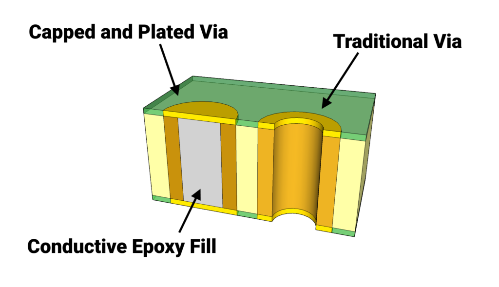
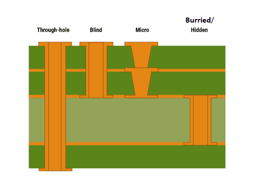
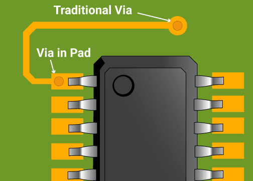
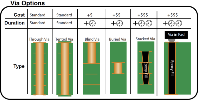
Considering the extra manufacturing cost and time for via-in-pad routing, if you prioritize speed over size reduction for your boards, then you should explore an alternative for your SMD routing and apply techniques to reduce manufacturing time for via routing. Instead of via-in-pad routing, you may opt to use vias between pads, which require more space. You may also consider capping or plugging the vias during fabrication, which will reduce the temperature impact within the via during assembly. However, the caps must be flat for proper SMD placement. Finally, instead of using a through hole, you may choose to use micro-vias, which don’t penetrate the entire board. However, if none of these alternatives suffice and size reduction remains your overriding concern, choose a manufacturer capable of optimizing your board size with via-in-pad routing.

Free PCB Request for Quotation (RFQ)

1. You can send email to us (tedchen163@yahoo.com). We will provide you with a
solution to make your PCB cost lower.
2. GoJGo receive your order,review the first,if there are questions,we will communicate with you
the first time and answer you about the lead time.
3. Our Engineering department will review this order with relevant departments,Produced in the best
process and in the shortest time.
4. Before shipment,we will talk with you about the shipping time and shipping method.

If you would like to customize your PCB type and place an order online, please click below to request a quotation.