This technology is mainly used in “Pay-in-pad” solutions and is also applicable to stacked non-interlaced (micro) vias. Via filling helps to facilitate additional routing traces among BGA vias. What’ s more, the filled and capped vias are also possible for blind vias.
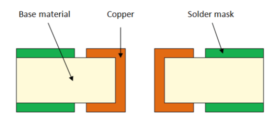
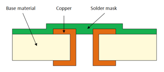
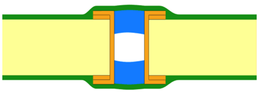
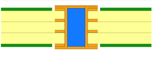
The easiest production method is to have all vias open from both sides, and then the vias will be clean without any contamination and solder mask. But this method has the risk of short circuits. The practical fabrication way is covering the vias with solder mask on both sides, which may exist a chance that the via-hole is not completely closed and remaining a small opening in the middle. And it may cause possible failures in the usage of the PCB if the chemicals get stuck in these small opening in subsequent processes.
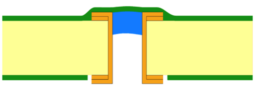
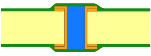
The most reliable method is filling the vias, but it is complicated and expensive. Each via covering type has its advantages and disadvantages. Customers can prepare their layouts according to the actually required standard of PCB assembly prototype or PCB mass production.