PCB Silkscreen
The graphics and text on PCB a circuit board is usually printed with a permanent non-conductive epoxy ink. The color is typically WHITE, although other colors may be available. Requirements are addressed in IPC-4781 QUALIFICATION AND PERFORMANCE SPECIFICATION OF PERMANENT, SEMI-PERMANENT AND TEMPORARY LEGEND AND/OR MARKING INKS.
I’ve never heard of a problem with Silkscreen as a material, except maybe some discoloration after high PCB reflow temperatures for RoHS compliant soldering. Silkscreen problems are almost always caused by circuit board DESIGNERS, so I’m going to take this opportunity to mention a few guidelines (which I will probably repeat in a later section, but worth repeating because designers often do not give silkscreen the attention it deserves!)
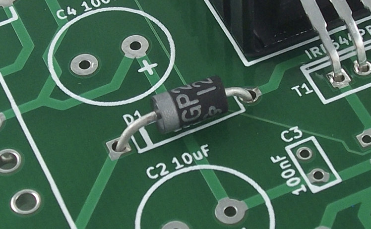
If silkscreen epoxy is printed over lands PCB or pads that will be soldered, it will melt into the solder joint during reflow and weaken the attachment. Therefore, silkscreen should always be printed on top of the mask material and never over solderable surfaces. Many CAD systems can clip the silkscreen away from exposed metal, but when creating library components be sure to keep the component outlines and polarity marks away from the pins (0.25mm) by default, and pay attention when moving or rotating reference designators or when adding text to PCB the final board design.
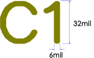
The width of silkscreen graphics can also be a problem. If too thin, PCB the fabricator will have problems in the screening or printing process and skips can occur. If too thick, the text may be too blurry to read. As components get smaller in size and circuit density continues to increase, it is sometimes very difficult to print silkscreen at all, but try to use line widths not less than 0.15 mm (6 mils), 0.18 mm to 0.20 mm is preferred PCB.
Solder pads should never be overprinted, because this may lead to problems during soldering, assembly, and with the E-Test. If we should detect an overprinted solder pad (spacing < 150μm), then Multi-CB reserves the right to remove the marking print at this location. Relevant for the definition of the solder pads is the solder pad exemption. The marking print is usually automatically clipped with a spacing of 100μm to the solder-stop edge.

Min. Character Width: ≥6mil
Characters width less than 6mil(0.153mm) will be unidentifiable.
Min. Character Height: ≥32mil
Characters height less than 32mil will be unidentifiable.

Tips for Silkscreen PCB Design
Default, all silkscreen layer will be processing. Please remove the extra characters and describe. If possible, try to remov unwanted silkscreen layer file.
* For GoJGo’s PCB board manufacture. Both side silkscreen is no additional cost.
Do not use silkscreen layer to defined any slot,outline layer or annular sign(annular mark). The right way is that you can use mechanical layer & keepOut layer (protel software), or add an new layer to define.

As discussed earlier, using a silkscreen PCB layout is an important aspect of board design and not including it can cause serious problems for PCB assembly and testing. The silkscreen is also used for labeling, which may include manufacturer information(such as serial number), testing certifications, model or serial numbers. In order to be effective and useful, the silkscreen must have clearly readable text, provide sufficient image resolution and, most importantly, be accurate. Here are a few tips to help you ensure that your silkscreen PCB layout can be used for its important roles in PCB assembly, testing and identification:
- Tip 1: Only use fonts approved by your CM as some fonts, although easily created in software, are difficult to generate during board manufacture.
- Tip 2: Use white or black instead of other colors to provide the best contrast with your board’s solder mask color.
- Tip 3: Make sure to follow your CM’s clearance and dimension guidelines. This will ensure that your silkscreen items do not get covered by components and are easily visible.
Free PCB Request for Quotation (RFQ)
1. You can send email to us (tedchen163@yahoo.com). We will provide you with a
solution to make your PCB cost lower.
2. GoJGo receive your order,review the first,if there are questions,we will communicate with you
the first time and answer you about the lead time.
3. Our Engineering department will review this order with relevant departments,Produced in the best
process and in the shortest time.
4. Before shipment,we will talk with you about the shipping time and shipping method.
If you would like to customize your PCB type and place an order online, please click below to request a quotation.