Comparison of several PCB surface finish types

As for the essential proceed in PCB production, the basic purpose of surface treatment is to ensure
good solderability or electrical properties. Since copper in nature tends to exist in the form of
oxides in the air, it is unlikely to remain as copper for a long time. Therefore, other treatment for
the copper is needed.

There are many kinds of surface treatments, and mainly shown with 5 ones, they are HASL, OSP, ENIG,
Immersion tin and Immersion silver.

HASL / Lead Free HASL

HASL is the predominant surface finish used in the industry. The process consists of immersing circuit boards in a molten pot of a tin/lead alloy and then removing the excess solder by using ‘air knives’, which blow hot air across the surface of the board.

One of the unintended benefits of the HASL process is that it will expose the PCB to temperatures up to 265°C which will identify any potential delamination issues well before any expensive components are attached to the board.

Advantages:

  • Low Cost
  • Widely Available
  • Re-workable
  • Excellent Shelf Life

Disadvantages:

  • Uneven Surfaces
  • Not Good for Fine Pitch
  • Contains Lead (HASL)
  • Thermal Shock
  • Solder Bridging
  • Plugged or Reduced PTH’s (Plated Through Holes)
Printed Circuit Board with HASL / Lead Free HASL Surface Finish

Electroless Nickel Immersion Gold (ENIG)

ENIG is a two layer metallic coating of 2-8 μin Au over 120-240 μin Ni. The Nickel is the barrier to the copper and is the surface to which the components are actually soldered to. The gold protects the nickel during storage and also provides the low contact resistance required for the thin gold deposits. ENIG is now arguably the most used finish in the PCB industry due the growth and implementation of the RoHs regulation.

Advantages:

  • Flat Surface
  • No Pb
  • Good for PTH (Plated Through Holes)
  • Long Shelf Life

Disadvantages:

  • Expensive
  • Not Re-workable
  • Black Pad / Black Nickel
  • Damage from ET
  • Signal Loss (RF)
  • Complicated Process
Printed Circuit Board with Electroless Nickel Immersion Gold (ENIG) Surface Finish

Immersion Tin

According to IPC, the Association Connecting Electronics Industry, Immersion Tin (ISn) is a metallic finish deposited by a chemical displacement reaction that is applied directly over the basis metal of the circuit board, that is, copper. The ISn protects the underlying copper from oxidation over its intended shelf life.

Copper and tin however have a strong affinity for one another. The diffusion of one metal into the other will occur inevitably, directly impacting the shelf life of the deposit and the performance of the finish. The negative effects of tin whiskers growth are well described in industry related literature and topics of several published papers.

Advantages:

  • Flat Surface
  • No Pb
  • Re-workable
  • Top Choice for Press Fit Pin Insertion

Disadvantages:

  • Easy to Cause Handling Damage
  • Process Uses a Carcinogen (Thiourea)
  • Exposed Tin on Final Assembly can Corrode
  • Tin Whiskers
  • Not Good for Multiple Reflow/Assembly Processes
  • Difficult to Measure Thickness
Printed Circuit Board with Immersion Tin Surface Finish

OSP / Entek

OSP (Organic Solderability Preservative) or anti-tarnish preserves the copper surface from oxidation by applying a very thin protective layer of material over the exposed copper usually using a conveyorized process.

It uses a water-based organic compound that selectively bonds to copper and provides an organometallic layer that protects the copper prior to soldering. It’s also extremely green environmentally in comparison with the other common lead-free finishes, which suffer from either being more toxic or substantially higher energy consumption.

Advantages:

  • Flat Surface
  • No Pb
  • Simple Process
  • Re-workable
  • Cost Effective

Disadvantages:

  • No Way to Measure Thickness
  • Not Good for PTH (Plated Through Holes)
  • Short Shelf Life
  • Can Cause ICT Issues
  • Exposed Cu on Final Assembly
  • Handling Sensitive
Printed Circuit Board with OSP / Entek Surface Finish

Gold – Hard Gold

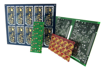
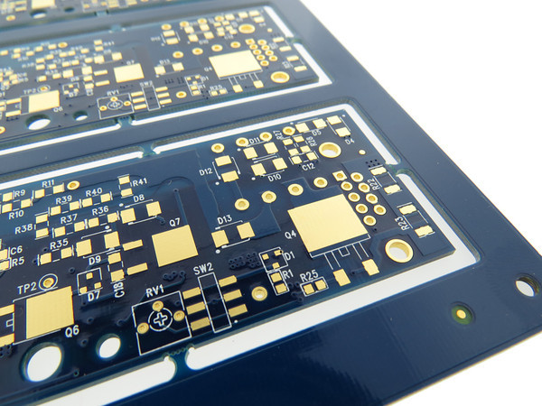
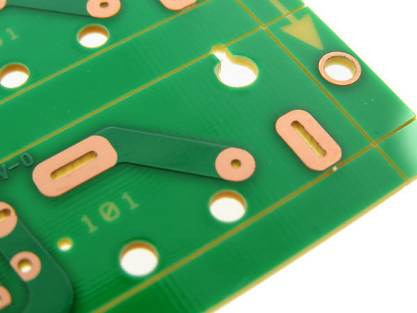
Hard Electrolytic Gold consists of a layer of gold plated over a barrier coat of nickel. Hard gold is extremely durable, and is most commonly applied to high-wear areas such as edge connector fingers and keypads.

Unlike ENIG, its thickness can vary by controlling the duration of the plating cycle, although the typical minimum values for fingers are 30 μin gold over 100 μin nickel for Class 1 and Class 2, 50 μin gold over 100 μin nickel for Class 3.

Hard gold is not generally applied to solderable areas, because of its high cost and its relatively poor solderability. The maximum thickness that IPC considers to be solderable is 17.8 μin, so if this type of gold must be used on surfaces to be soldered, the recommended nominal thickness should be about 5-10 μin.

Advantages:

  • Hard, Durable Surface
  • No Pb
  • Long Shelf Life

Disadvantages:

  • Very Expensive
  • Extra Processing / Labor Intensive
  • Use of Resist / Tape
  • Plating / Bus Bars required
  • Demarcation
  • Difficulty with Other Surface Finishes
  • Etching Undercut can Lead to Slivering / Flaking
  • Not Solderable Above 17 μin
  • Finish Does Not Fully Encapsulate Trace Sidewalls, Except in Finger Areas
Printed Circuit Board with Gold – Hard Gold Surface Finish

Choose the Right Finish for Your PCBs

GoJGo offers a wide range of other finishes such as ENEPIG, Wire Bondable Soft Gold, and others, depending on the application.  

Above types of PCB surface finish are commonly used in GoJGo. Besides, there are Immersion silver,Immersion Tin,Hard Gold,Nickel palladium (ENEPIG) and so on. Now, according to your own requirements, you can choose a suitable surface finish type.

Free PCB Request for Quotation (RFQ)

1. You can send email to us (tedchen163@yahoo.com). We will provide you with a
solution to make your PCB cost lower.
2. GoJGo receive your order,review the first,if there are questions,we will communicate with you
the first time and answer you about the lead time.
3. Our Engineering department will review this order with relevant departments,Produced in the best
process and in the shortest time.
4. Before shipment,we will talk with you about the shipping time and shipping method.

If you would like to customize your PCB type and place an order online, please click below to request a quotation.