Services
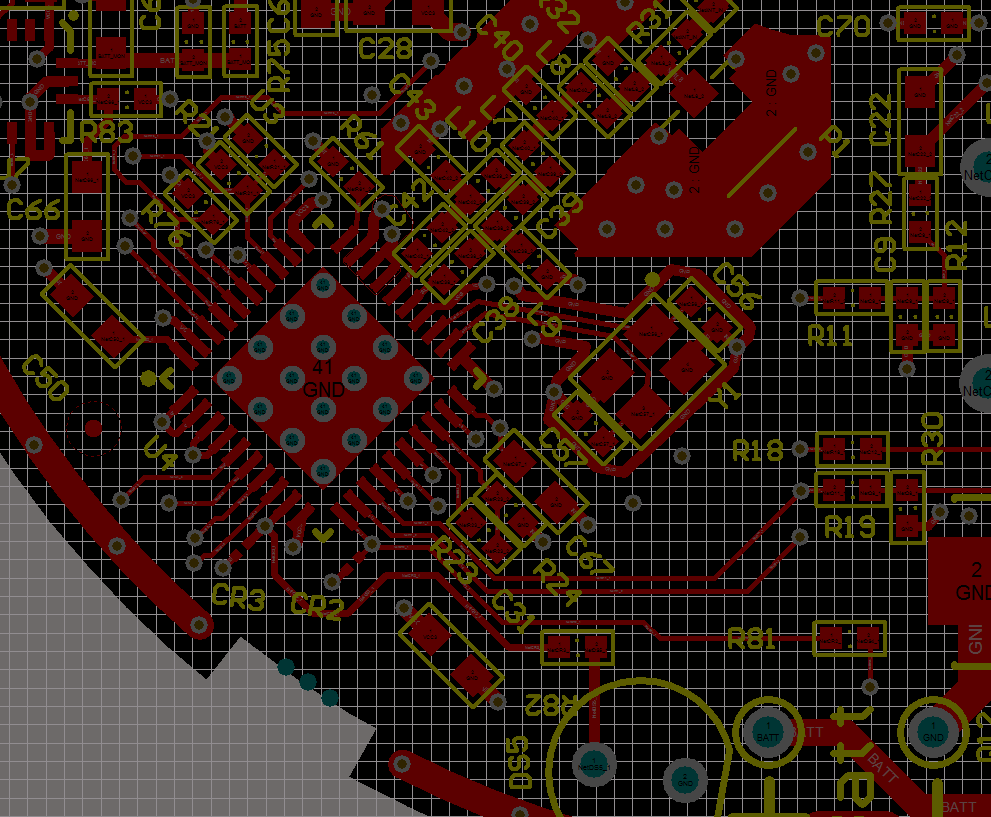
PCB Design and Layout
PCB Layout is a two way process. Effective communication between you and us is key to a successful project. We welcome your questions and suggestions.
HOW WE WORK WITH YOU
Effective communication is the key to success for the projects. We appreciate files and main cases through email and details on Skype. Contact information listed on the right upper corner of the sign in page.
WHAT WE NEED FOR DESIGN & LAYOUT
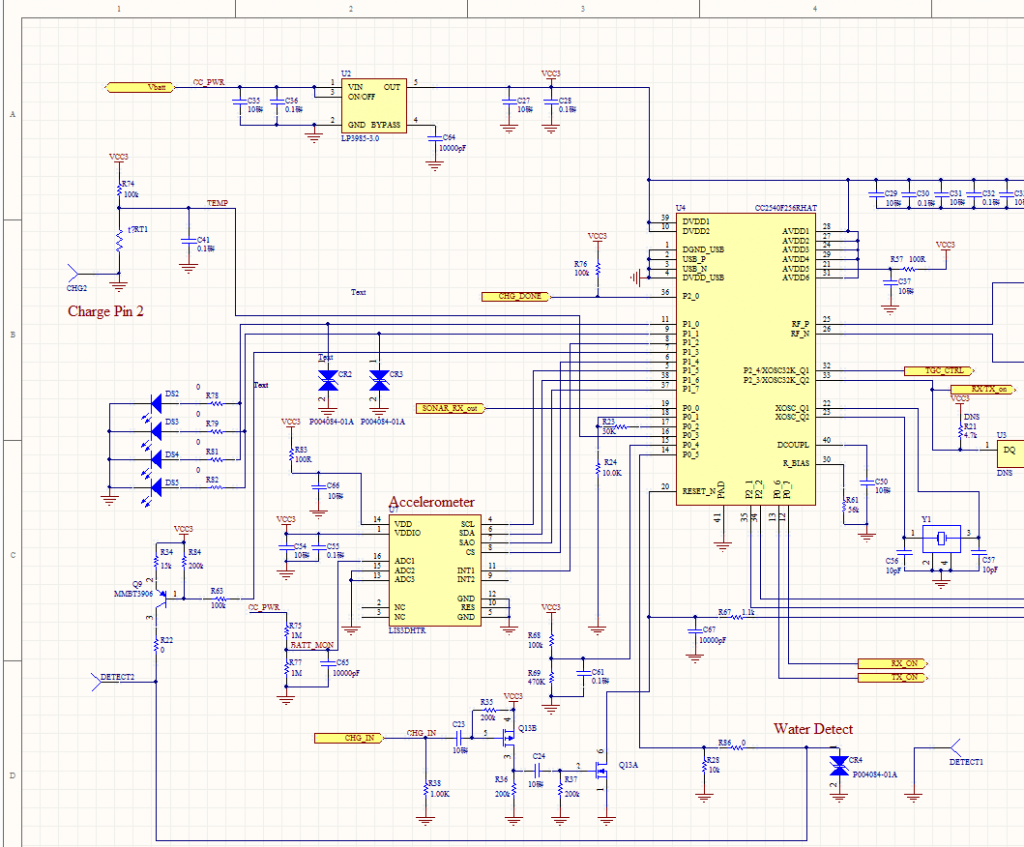
1)Schematics(.DSN and .SCH suffixes )
2)DXF structure drawing (2D drawing in AutoCAD format, used to position the device and build board size)
3)The component specification (the specification must be with the device size diagram for the establishment and physical one-to-one corresponding package)
4)Special requirements
WHAT SOFTWARE WE USE
Cadence Allegro, Mentor PADS, Altium Designer and Protel DESIGN BASIS Design Rule, Design Instructions, and Customer’s Requirements
WHAT FILES WE CAN SEND TO YOU
Design source files, Gerber files, Centroid file and Designator Diagram Simply give us a quote. We are here to help.