| Item | Capability | Details | |
| Layer | 1-6 layer | 1-6 copper layers PCB prototypes (Don't support Blind/Buried Vias) | |
| Controlled Impedance PCB | 4/6 layer | Impedance control is available | |
| Material | FR4, Aluminum, Copper base, Flexiable PCB | FR-4 Standard Tg 130°C, FR4-High Tg 150°C, FR4-High-Tg 160°C. Metra core PCB: Aluminum, Copper base Rogers, HDI Flexiable PCB, Rigid-Flex Board |
|
| Max. Dimension | 400x500mm | For Single&Double Layer, the maximum dimension is 400x500mm; For Multi Layer PCB, the maximum dimension is 300x300mm. | |
| Dimension Tolerance (Outline) | ±0.2mm | ±0.2mm for CNC routing, and ±0.2mm for V-scoring | |
| Solder Mask | LPI | Liquid Photo-Imageable Solder Mask is the most common mask type. No extra fee for different color of solder mask. |  |
| Thickness | 0.4--2.0mm | 0.4/0.6/0.8/1.0/1.2/1.6/2.0mm | |
| Thickness Tolerance ( Thickness≥1.0mm) | ± 10% | e.g. For the 1.6mm board thickness, the finished board thickness ranges from 1.44mm(T-1.6×10%) to 1.76mm(T+1.6×10%) | |
| Thickness Tolerance ( Thickness<1.0mm) | ± 0.1mm | e.g. For the 0.8mm board thickness, the finished board thickness ranges from 0.7mm(T-0.1) to 0.9mm(T+0.1). | |
| Finished Outer Layer Copper | 1 oz/2 oz (35um/75um) | Finished outer layer copper weight is 1oz or 2oz |  |
| Finished Inner Layer Copper | 0.5 oz (17um) | Finished inner layer copper weight is 0.5 oz only |  |
| Min. Trace | 3.5mil | For Single&Double Layer PCB, the minimum trace width is 5 mil; For Multi Layer PCB, the minimum trace width is 3.5mil. |  |
| Min. Spacing | 3.5mil | For Single&Double Layer PCB, the minimum spacing is 5 mil; For Multi Layer PCB, the minimum spacing is 3.5mil. |  |
| Min. Via hole size | 0.2mm | For Single&Double Layer PCB, the minimum via hole size is 0.3mm; For Multi Layer PCB, the minimum via hole size is 0.2mm. |  |
| Min. Via diameter | 0.45mm | For Single&Double Layer PCB, the minimum Via diameter is 0.6mm; For Multi Layer PCB, the minimum via diameter is 0.45mm. |  |
| Via To Trace | ≥5mil | Minimum distance between via(plated holes) and trace is 5mil. |  |
| Drill Hole Size | 0.2--6.3mm | Min. drill size is 0.2mm, Max. drill size is 6.3mm. |  |
| Hole Size Tolerance | ±0.08mm | e.g. For the 0.6mm hole, the finished hole size between 0.52mm to 0.68mm is acceptable. | |
| Annular Ring | ≥3mil | Annular ring surrounded by traces should be equal to or larger than 3mil |  |
| Min. Character Width | ≥6mil | Characters width less than 6mil(0.153mm) will be unidentifiable. |  |
| Min. Character Height | ≥32mil | Characters height less than 32mil will be unidentifiable. |  |
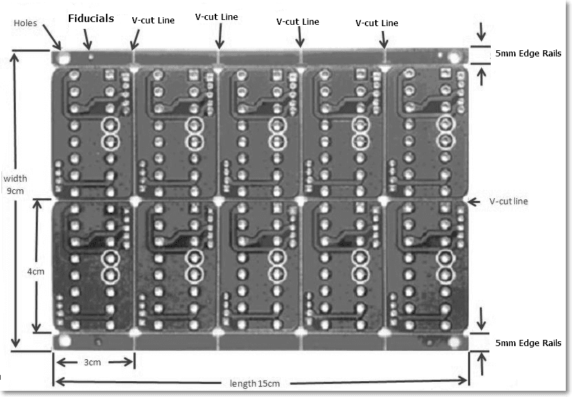
| Trace to Outline | ≥0.2mm | Ship as individual board(Routing): Trace to Outline ≥0.2mm;Ship as panel with V-scoring: Trace to V-cut line ≥0.4mm | 
 |
| Panelization without space | 0mm |  |
|
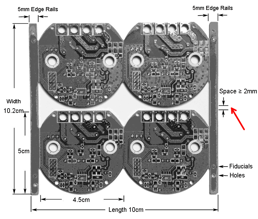
| Panelization with space | ≥2mm | Make sure the space between boards should be ≥2mm, otherwise it will be hard to process for routing. |  |
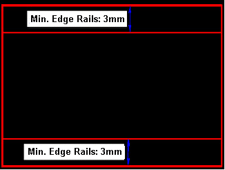
| Min. Edge Rails | 3mm |  |
|
| Copper Hatching with Pads | Hatch | We will apply Copper Hatching if your PCBs designed with Pads. | |
| Slot Drawing with Pads | Outline | Please use Outline to design if there are many non-plated (NPTH) holes. | |
| Protel/dxp Solder Layer | Solder Layer | Do not mistake the Paste Layer as Solder Layer. | |
| Protel/dxp Outline Layer | Keepout Layer/Mechanical Layer | Only choose one from Keepout Layer or Mechanical Layer as outline. | |
| Min. Half Hole Diameter | 0.6mm | Half hole is a special technology, so half hole diameter should be greater than 0.6mm. | |
| Soldermask Bridge/ Blind and buried vias | Soldermask Bridge/Blind and buried vias are not available now |

