PCB BGA

A ball grid array (BGA) is a type of surface-mount packaging used for integrated circuits. BGA packages are used to permanently mount devices such as microprocessors. A BGA can provide more interconnection pins than can be put on a dual in-line or flat package, each pin is provided with a solder ball. All connections are distributed in a uniform surface grid or matrix on the component. The whole bottom surface of the device can be used instead of just the perimeter.


The leads are also on average shorter than with a perimeter-only type, leading to better performance at high speeds.


Soldering of BGA devices requires precise control and is usually done by automated processes. BGA devices are not suitable for socket mounting.

The advantage of BGA:

1. Efficient use of PCB space. Using BGA packages means fewer component involvement and smaller footprints, it is also help to save space for custom PCBs, which greatly increases the effectiveness of PCB space.

2. Improve thermal and electrical performance. Due to small size of PCB base on BGA package, heat dissipation is more easily. When silicon wafer is mounted on top, most heat can be transmitted down to the ball grid. When silicon wafer is mounted on the bottom, the backside of the silicon wafer connect to the top of the package and is considered to be one of the best heat dissipation methods. The BGA package has no pins that can be bent and broken, which makes it stable enough to ensure large-scale electrical performance.

3. Improve manufacturing profit based on welding improvement. Most BGA package pads are large, which makes large area soldering easier and more convenient. As a result, the manufacturing speed of PCB increased with the increase of manufacturing yield. In addition, when using larger pads, it is easily to re-work.

4. Less damage . BGA leads consist of solid solder balls that are not easily damaged during operation.

5. Reduce costs. All advantages shown above help to reduce costs. Efficient use of PCB space provides opportunities to save material, while improving thermoelectric performance helps ensure the quality of electronic components and reduce defects.

GoJGo BGA technology:

The usually BGA technology of GoJGo are minimum size 0.3mm, the minimum distance to circuit line is 0.2mm,the minimum distance between two BGA is 0.2mm. If you need higher requirement, please make a note.

BGA Design Guidelines

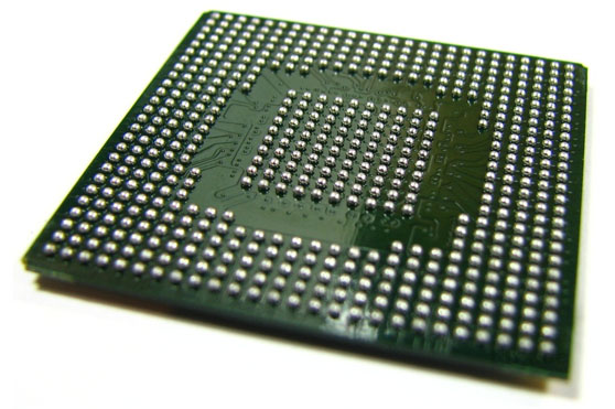
I was asked by many PCB designers about BGA design guidelines, say ball PAD size, pitch size, annular ring, layer counts, solder mask opening, etc. There is no ready answer for it, because every BGA is different from one another, yet there are some rules and tips to follow to make better results. In this article, I am going to introduce them step by step.

There are 4 parts in the article as showing below:

1. The advantages of using BGA

2. How to avoid BGA design mistakes

3. BGA design rules

4. BGA PCB feature definitions


1. The advantages of using BGA

A BGA package is more advantageous at design layout because it provides increased functionality at the same package size compared to the Quad Flat pack (QFP). It improves the ratio of pin count to board size, hence providing more connections and increased area for routing.

A BGA package also offers better thermal and electrical performance. It does that by providing ground planes for a low impedance power system and controlled impedance on traces. 

BGAs also offer reduced package thickness than those with pins. Moreover, BGA balls are considerably stronger than QFP leads and therefore can tolerate rough handling. This can potentially reduce the cost of ownership by virtue of their re-workability.

2. How to avoid BGA design mistakes

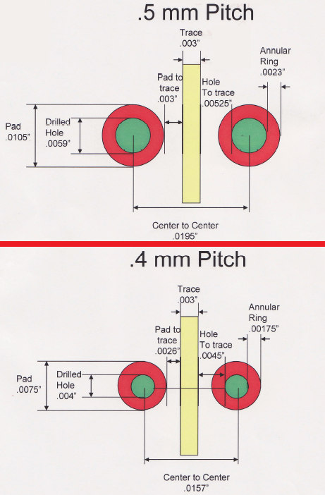
Today’s smaller packaging can create confusion to PCB designers. When designing with BGA with pitch sizes of 0.5mm and above, there are certain rules of thumb related to pad sizes and solder mask opening. One is to maintain pad size to about 85 % of a BGA’s ball size. Another is to use a non-solder mask defined (NSMD) pad. In this case, the solder mask is larger than the BGA pad.

The solder mask is usually opened to a diameter of about the ball size of the BGA. The recessed solder mask provides stress relief to the NSMD pad during reflow. In short, it creates a protective barrier and lets solder go around it.

Then, there are solder mask defined (SMD) pads, which are used for 0.4mm and below pitch BGA PCB designs. NSMD and SMD pad definitions and photos are shown in the bottom of this article. In the SMD pad case, the solder mask opening is smaller than the pad size. Better yields and results are achieved for these particular PCB designs.

Below are some tips to avoid BGA design mistakes.

1. Using NSMD pad sizes for 0.4mm pitch BGA PCB design may provide favorable results at low volumes, but chances are low yields result at high-volume production runs.

2. Keep in mind that ball size of 0.4mm pitch BGAs are smaller than those of 0.5mm pitch BGAs. Reducing pad size further may cause an insufficient solder-able area on the BGA pads. This can lead to PCBs being rejected at assembly inspection or latent failures in the field.

3. Bridging can be created between pads when using NSMD pads for 0.4- and 0.3mm pitch BGAs. Bridging is created because there’s not enough solder mask webbing between pads.

4. Since pad sizes are so small, and there is no solder mask webbing to provide adhesive strength, the pad may peel off, during reflow, or in the field. It’s best to have no trace between two BGA pads. Having them introduces shorts at pitches of 0.4mm and smaller on external layers.

5. On internal layers, there should be just one trace between pads. Also, PCB fabrication problems surface when running multiple and thin 2 to 3 mil traces between two BGA pads.

6. Make all vias solder mask covering; for the vias at BGA area, they should be via plugged. This is better for your assembly purpose.

3. BGA design rules

Figures are easier and better understandable than words, See below photo and diagram. 

Conversion between mm and mils

0.075mm = 3 mils (0.003”)

0.1mm = 4 mils (0.004”)

0.125mm = 5 mils (0.005”)

0.2mm = 8 mils (0.008”)

0.4mm = 16 mils (0.016”)

0.45mm = 18 mils (0.018”)

0.5mm = 20 mils (0.020”)


4. BGA PCB feature definitions

Pitch-distance between the center of one ball to the center of the next one.

Via diameter – the full width of the via annular ring, also called PAD

Ball pads-Also called BGA “lands”. This is the copper that the BGA ball solders to.

Micro via – a via that is laser drilled.

HDI – High Density Interconnect. This is the type of board that uses very small vias like micro vias. When a board uses micro vias it is called an HDI board.

The Quad Flat Package, or Quad Flat Pack, QFP, is a package used for surface mount, SMD integrated circuits

NSMD pad – Non-Solder Mask Defined ball pad. This kind of pad has an opening that is defined only by the size of the ball pad. The solder mask is applied around the ball pad and does not cover it. This kind of pad is more popular lately and has the advantage of increased ball adhesion because the ball flows around the sides of the ball pad and grips on the top and the sides. This kind of pad is usually recommended for BGA designs 0.5mm and above.

SMD pad – Solder Mask Defined ball pad. This kind of pad has a large copper area, but the solder mask covers the edges, so the opening is known as solder mask defined. This kind of pad is sometimes best for very small pitch pads where ball shorting is an issue. 

Free PCB Request for Quotation (RFQ)

1. You can send email to us (tedchen163@yahoo.com). We will provide you with a
solution to make your PCB cost lower.
2. GoJGo receive your order,review the first,if there are questions,we will communicate with you
the first time and answer you about the lead time.
3. Our Engineering department will review this order with relevant departments,Produced in the best
process and in the shortest time.
4. Before shipment,we will talk with you about the shipping time and shipping method.

If you would like to customize your PCB type and place an order online, please click below to request a quotation.