Impedance Control PCB Manufacturing

What is Impedance?

Impedance is the effective resistance of an electric circuit to alternating current, arising from the combined effects of Ohmic Resistance and Reactance. Transmission lines are for signal delivery in PCB and its Impedance depends on the length and width of the lines and also the insulation base material called substrate.

What is Control Impedance?

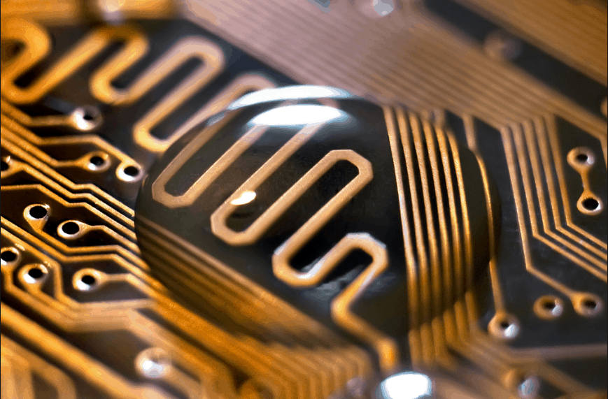
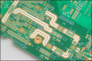
Unless you have carefully designed the trace and its environment, impedance is typically “uncontrolled”, meaning that impedance will vary in value from point to point along the trace.

At high frequencies, PCB traces do not behave like simple connections, controlled impedance helps us ensure that signals are not degraded as they route around a PCB.

Essentially, controlled impedance is the matching of substrate material properties with trace dimensions and locations to ensure the impedance of a trace’s signal is within a certain percentage of a specific value. Control impedance boards provide repeatable high-frequency performance.

Applications of Control Impedance PCB Boards

Controlled Impedance should be considered for PCBs used in fast digital applications such as:
– Telecommunications
– Computing 100MHz and above
– High Quality Analog Video
– Signal Processing
– RF Communication

Impedance control parameter

It is very convenient for customers to conduct impedance matching design according to the standard laminated structure and related parameters, the PCB will be produced in accordance with the following stack up strictly.  

Please don’t hesitate to contact us by email if you need more information about impedance control solutions. 

Refer to the following example. 


Controlled Impedance PCB Parameters and Stack up

1.Prepreg dielectric constant:

Prepreg type

Dielectric constant

2313

4.05

2.Solder mask Parameters

Solder mask thickness over the laminate

Solder mask thickness over traces

Solder mask dielectric constant

0.8mil

0.5mil

3.8

  • 4 layer board , 1.0 mm board thickness, 2313 Stackup:

Layer

Material Type

Thickness


Top Layer1

Copper

0.035 mm


Prepreg

2313*1

0.1 mm


Inner Layer2

Copper

0.0175 mm

0.7 mm (with copper core)

Core

Core

0.665 mm

Inner Layer3

Copper

0.0175 mm

Prepreg

2313*1

0.1 mm


Bottom Layer4

Copper

0.035 mm

 
  • 4 layer board , 1.6 mm board thickness, 2313 Stackup:

Layer

Material Type

Thickness


Top Layer1

Copper

0.035 mm


Prepreg

2313*1

0.1 mm


Inner Layer2

Copper

0.0175 mm

1.3 mm (with copper core)

Core

Core

1.265 mm

Inner Layer3

Copper

0.0175 mm

Prepreg

2313*1

0.1 mm


Bottom Layer4

Copper

0.035 mm


Free PCB Request for Quotation (RFQ)

1. You can send email to us (tedchen163@yahoo.com). We will provide you with a
solution to make your PCB cost lower.
2. GoJGo receive your order,review the first,if there are questions,we will communicate with you
the first time and answer you about the lead time.
3. Our Engineering department will review this order with relevant departments,Produced in the best
process and in the shortest time.
4. Before shipment,we will talk with you about the shipping time and shipping method.

If you would like to customize your PCB type and place an order online, please click below to request a quotation.