
What is the high frequency PCB
High-frequency board refers to the special circuit board with high electromagnetic frequency, which is
used for PCB in the field of high frequency (frequency greater than 300MHz or wavelength less than 1m)
and microwave (frequency greater than 3GHZ or wavelength less than 0.1m). Generally speaking, the
high-frequency board can be defined as a circuit board with a frequency above 1GHz. To cope with the
high-frequency and high-speed requirements of 5G, development of PCB materials will focus on lower
dielectric constant (Dk) and dielectric loss (Df) and low humidity to prevent excessive water
absorption and quality uniformity.
A High-Frequency PCB Requires the Use of Specialized Materials
1. High frequency PCB must use low water absorption of the substrate if use high water absorption will
be affected by moisture dielectric constant (Dk) and dielectric loss (Df).
2. The thermal expansion coefficient of the high speed high frequency PCB substrate and copper foil
must be consistent, otherwise, it will cause copper foil separation.
3. High frequency signal PCB substrate dielectric constant (Dk) must be small and stable. Generally
speaking, the smaller the better, because of the signal transmission rate and the square root of the
material dielectric constant is inversely proportional. The high dielectric constant is easy to cause
signal transmission delay.
4. PCB for high frequency substrate material dielectric loss (Df) must be small. Dielectric loss (Df)
mainly affects the quality of signal transmission, the smaller the dielectric loss, the smaller the
signal loss.
5. High frequency PCB materials also require high heat resistance, chemical resistance, impact
strength, and peel strength
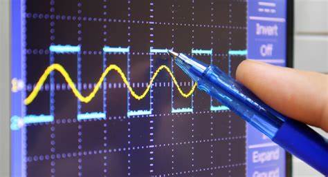
At the same time, we should also consider the signal transmission and crosstalk and other electrical
problems when the high frequency signal PCB design.
Special materials are required to achieve the high frequency provided by this type of printed circuit board – any changes in the Er value of these materials can affect the impedance of the board. Many PCB designers turn to Rogers dielectric material for its lower dielectric loss, reduced signal loss, lower cost of circuit fabrication and better suitability for fast-turnaround prototyping applications.
Apart from choosing the appropriate PCB material and determining the correct the value of the Er, designers should take parameter such as conductor width and spacing, substrate constant into consideration. These parameters must be exactly specified and implemented with the highest level of process control.
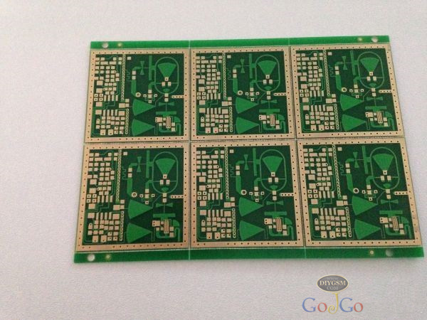
Why choose GoJGo high frequency PCB
GoJGo is a professional PCB prototype manufacturer with 15 years of experience in China. Master all
kind of high-frequency materials and manufacturing requirements, rich experience in various high-
frequency circuit design, material brand, specifications, thickness (mm), dielectric constant (ER).
Cooperate with famous brands of advanced high-frequency materials to ensure the quality of your
products
Common stock sheet and parameters
| Material | Dielectric Constant |
| RO4350B | 3.48±0.05@10 GHz |
| RO4003C | 3.38±@10 GHz |
| Ro3003 | 3.00±0.04@10 GHz |
| Ro3010 | 10.2±0.03@10 GHz |
| RT5880 | 2.20±0.02@10 GHz |
Mature process of PCB technology and rich production experience
High-frequency board performance and production process is special, in order to produce the best products, the manufacturer must have rich experience in processing production. GoJGo high-frequency PCB manufacturing is controlled from the following points
A、High frequency microwave board is used to transmit high frequency signals. The impedance control requirements of finished PCB wires are strict. The line width tolerance of the printed circuit board is usually ±0.02mm (even ±0.015mm).Therefore, from the perspective of engineering data, our engineers will compensate the line width according to different copper thickness, and the etched board will measure the line width 100% to confirm whether it is within the tolerance range.
B、The high-frequency signal PCB design transmits high-frequency signal rather than current. Pit, notches, pinholes and other defects in the circuit line will affect the transmission effect, and any such minor defects are not allowed in the high-frequency PCB layout. Therefore, after the film is drawn, it must be checked to ensure that there are no pinholes or gaps in the film. The most difficult procedure of high-frequency board fabrication is chemical copper sinking. All holes must have copper and no blank. GoJGo adopts Plasma method, which is to inject carbon tetrafluoride (CF4) or argon (Ar2) nitrogen (N2) and oxygen (O2) gas between two high-pressure electrodes under the vacuum environment. The printed board is placed between two electrodes, and the Plasma is formed in the cavity, so as to remove the drilling dirt and dirt in the hole.
C、Solder resistance thickness is also strictly controlled and lines solder mask too thick or too thin for several microns can be disqualified.
D、The final destructive test must be carried out in manufacturing: thermal shock 288℃, 10 seconds, 1~3 times, to ensure no separation of hole wall.
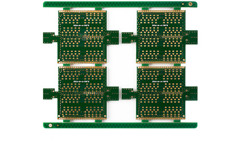
Superb process capability, tailor-made for you exclusive technology
A、High frequency hybrid printed circuit board.
B、8mm finished thickness high frequency PCB.
C、Copper base, ceramic base high frequency PCB.
D、Surface finish: ENIG, Gold plating, immersion Tin, immersion Sliver, Sliver plating, HASL, OSP, ENIG+OSP.
Advanced production equipment to ensure the processing accuracy of each piece of HF PCB
A、Advanced plasma cleaning machine and laser exposure machine and other process equipment and testing equipment can ensure the line and hole processing accuracy.
B、Introduction of ultra-thick, ultra-long circuit board processing equipment, meet the requirements for the communication industry various specifications of high-frequency PCB design and processing.
If you would like to customize your PCB type and place an order online, please click below to request a quotation.