
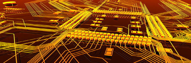
What is the HDI PCB
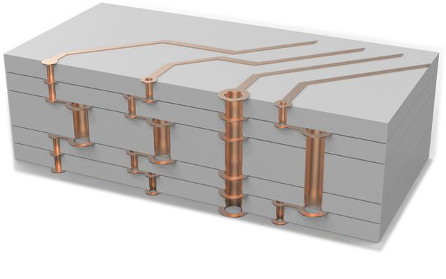
HDI is the acronym of High-Density interconnector, which is a technique for producing PCB, HDI in PCB
mainly includes Micro-blind hole technology. HDI PCB prototype has the features as follows:
1. Saving the cost of multi-layer PCB: when the PCB density increases to eight layers, the cost of HDI
PCB stack up will be lower than the cost of traditional stack-up process.
2. Increasing the line density to make the product more high precision.
3. Good heat dissipation and higher weldability.
Meanwhile, HDI is needed in all around the world. Different layouts have a great impact on the
price of HDI PCB, generally, we need to do a good plan before HDI PCB design so that enhancing good
performance and lower the HDI PCB cost.
Why choose GoJGo HDI PCB
HDI PCB factory of GoJGo has the capability to process mass production based on HDI micro-holes. it
also has rich experience in different HDI PCB fabrication for different HDI PCB market applications.
1. Top technical team, superb HDI technology
A、All the staff is professional HDI PCB manufacturers with 3-12 years’ experience in, so we ensured
the high stability and reliability of HDI products from the technical level.
B、The high precision back drilling technology can reduce the equivalent series inductance through the
hole to ensure the product signal transmission integrity.
2. Excellent technical ability to meet the HDI PCB producing requirements.
| Feature | Capability | |
|---|---|---|
| Layer count | 1~24 | |
| HDI Stack up | 1+N+1,2+N+2,3+N+3(with copper filling) | |
| Final board thickness | 0.15-3.2mm | |
| Aspect Ratio | Laser via PTH | 3:4 10:1 |
| Copper thickness | 1/3~6oz | |
| Impedance Control | Single Ended Differential | +/- 10% +/- 10% |
| Line/Space | Inner Layer External Layer | 2.5/2.5mil 2.5/2.5mil |
| Min Drill Bit size | 8mil | |
| Hole size tolerance | PTH NPTH | +/-3mil +/-2mil |
| Hole Position Tolerance | +/-2mil | |
| Profile Tolerance | Punching Routing | +/-3mil +/-4mil |
| Solder mask | Line to PAD Registration | 4mil +/-2mil |
| Warpage | 0.5% | |
| Surface Finish | HASL(LF HASL) ENIG OSP Immersion Tin Immersion Silver Hard Gold Plating Peelable Mask Carbon ink | SMD 40-2000u”, GND 30-800u” Au 1-5u”, Ni 80-200u” 0.8-1.2um 0.15-0.45um Au 1-50u”, Ni 80-200u” 5mil 0.3mil |
3. Advanced automatic production equipment and precision inspection equipment.
A、Equipping with a full range of surface treatment production line for HDI products.
B、Our company introduced automatic V-cut machine, German stack-up machine, Mitsubishi laser drilling
machine, Hitachi mechanical drilling machine, automatic exposure machine, LDI, AOI.
4. Rigorous quality control system to ensure 100% qualified rate of shipment.
A、Strictly in accordance with IPC standard control, to ensure 100% qualified rate of shipment.
B、Imported German advanced temperature cycle inspection equipment to ensure high reliability and
stability.
C、Strictly implement quality PDCA processes to continuously improve product performance.
How to order the HDI PCB
1. You can click the button as shown below in the lower right corner of GoJGo website,contact our customer service representative, or directly send the file to our email tedchen163@yahoo.com.
2.GoJGo will review your order as soon as possible after receiving it. If there is any problem, we will contact you immediately, on the contrary, if there is no problem, we will send you the quotation and delivery date.
If you would like to customize your PCB type and place an order online, please click below to request a quotation.