What Are Gold Fingers?

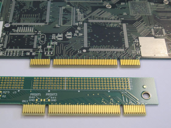
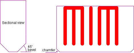
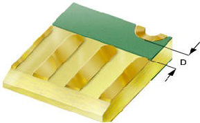
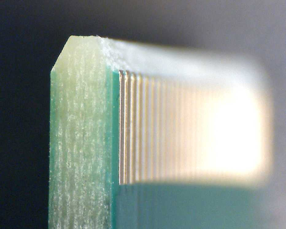
Gold fingers are the gold-plated columns that you see along the connecting edges of Printed Circuit Boards (PCBs). The purpose of gold fingers is to connect a secondary PCB to the motherboard of a computer.

PCB Gold Fingers are also used in various other devices that communicate via digital signals, such as smartphones and smartwatches. Gold is used for the connecting points along a PCB because of the alloy’s superior conductivity.

Other names to call a Gold finger PCB are Gold Connector, Edge Connector, Edge-Board Connector, Connector Finger, Contact Fingers, Gold Taps or Gold Tips.

Gold Fingers PCB Board

The gold finger bevel default value: 45 angle, As following figure. The default plating for gold finger does not support the hard gold.

How are gold fingers applied?

Gold fingers can be used for many different things. Their use would be based on the designer’s purpose. Some common applications of gold fingers are:

  • Provide an interconnection point for transferring network data.
  • A place for attaching daughter boards or specialized adapters.
  • Connect external components to the prototype PCB.
  • Function as an audio adapter.
bevel/chamfer edge
bevel/chamfer edge

Are there specific design specifications?

Yes. As we mentioned previously, there are some specifications depending on the need and use of the board. However, despite this, there are some design rules that must be followed no matter the board’s intended purpose. This includes:

  • No plated through holes can be included anywhere near the gold fingers.
  • No soldermask or screen printing can be included near the gold fingers.
  • The gold fingers should always be placed facing outward of the board’s center.

Enquiry

If you are interested in learning more about how these interesting little gold fingers work in the world of printed circuit boards, please contact our professionals today.

Free PCB Request for Quotation (RFQ)

1. You can send email to us (tedchen163@yahoo.com). We will provide you with a
solution to make your PCB cost lower.
2. GoJGo receive your order,review the first,if there are questions,we will communicate with you
the first time and answer you about the lead time.
3. Our Engineering department will review this order with relevant departments,Produced in the best
process and in the shortest time.
4. Before shipment,we will talk with you about the shipping time and shipping method.

If you would like to customize your PCB type and place an order online, please click below to request a quotation.