PCB Sideplating / Edge plating / Castellation

1. The definition of Sideplating

 Sideplating  is actually the metalization of the board edge in PCB filed. Edge plating、Border plated、plated contour、side metal, these words can be used too to describe same function. 

2. Sideplating Process

   Drilling – Milling plated Slots – Cleaning –  Copper sink

3. Pictures to show the finished board’s sideplating

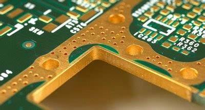
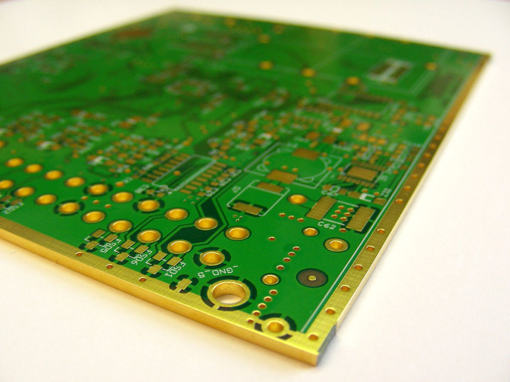
4. Possible applications of sideplating:

4.1 Improvement of EMC performance by shielding the inner region of multilayers (eg for HF circuit boards

4.2 Cooling function with the edge as additional cooling surface, where an active heat dissipation can be used

4.3 Housing connection

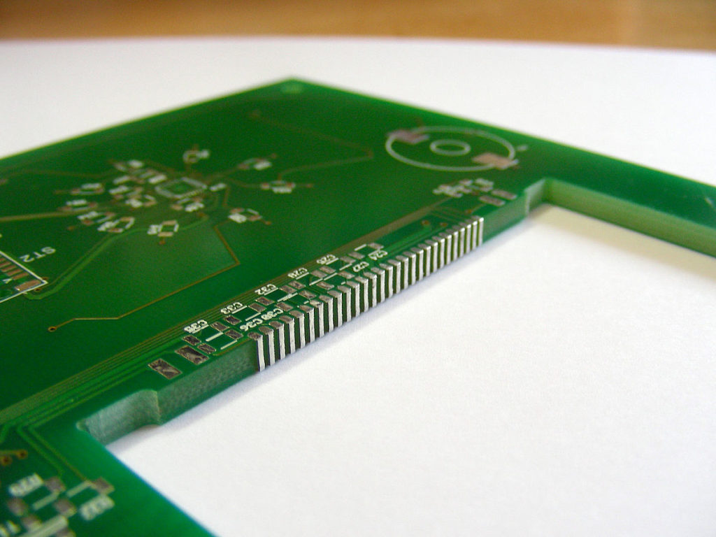
4.4 Board-on-Board connection (see plated half-holes)

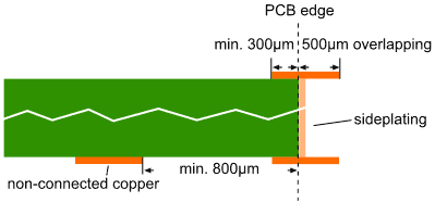
5. Design Parameters

To guarantee the producibility of the sideplating, the metallized area must be defined using overlapping copper (copper surface, pads, or tracks) in the CAD layout. Minimum overlap:500mm.

On the connected layer, min 300um of connected copper must be defined.

On non-connected layers, the copper should have gap of min. 800um from the outer contour.

Usually , we recommend customers to make immersion gold for edge plating.  When design the solder mask layer, it should be solder mask opening in the file. Also you can show us some texts to show the detailed requirements.

Edge Plating/castellation

GoJGo offers printed circuit board fabrication facility, allowing us to overcome many problems common in the industry. This includes proper execution of PCB edge castellation, where we can keep quality to tight tolerances for edge plating, even after profiling.

You might have heard this concept called “edge plating” or “castellation,” which is the copper plating that runs from the top to the bottom surfaces of a PCB, and runs along at least one of the perimeter edges. PCB edge castellation ensures a strong connection through the board and limits the chance of equipment failures, especially in controlling protections for small form factor boards and sub-motherboards.

Outter sideplating
Inner sideplating

Edge Plating PCB Process

Circuit board fabrication for edge soldering requires precision handling and faces many challenges around how plated edges are prepared and the lifetime adhesion of the plated material.

GoJGo has established industry practices and uses other optimum standards to ensure that our PCB edge castellation thoroughly prepares edge surfaces, applies the plated copper for immediate adhesion and processes the board to ensure long-term adhesion of every layer.

By using a controlled process in our circuit board fabrication for edge soldering, we can limit any potential hazard for through-holes and half-holes on the edge. The most significant concern is the creation of burrs, which will lead to the failure of mission-critical parts and can damage your equipment.

Applications

Edge plating circuit boards are common in many industries, and edge plating is a common practice. You’ll find PCB edge castellation (or edge plating PCB) applied in many cases, including:

  • Improving current-carrying capabilities
  • Edge connections and protection
  • Edge soldering to improve fabrication
  • Better support for connections such as boards that slide into metal casings

Please note that edge plating on printed circuit boards is a very simple addition in many cases, but it requires specialized equipment and training. It’s an option for many different boards, but we always recommend taking this type of request to a manufacturer who has an established reputation of circuit board castellation.

We’ll be able to perform the right checks to keep everything safe. For example, circuit board castellation should never cause the internal power planes to come to the edge of the board, because it can short the edge plating. When you travel, always mind the gap. When we perform circuit board fabrication for edge soldering, we always make sure there’s a gap before the edge plating.

Free PCB Request for Quotation (RFQ)

1. You can send email to us (tedchen163@yahoo.com). We will provide you with a
solution to make your PCB cost lower.
2. GoJGo receive your order,review the first,if there are questions,we will communicate with you
the first time and answer you about the lead time.
3. Our Engineering department will review this order with relevant departments,Produced in the best
process and in the shortest time.
4. Before shipment,we will talk with you about the shipping time and shipping method.

If you would like to customize your PCB type and place an order online, please click below to request a quotation.