Blind vias and Buried Vias

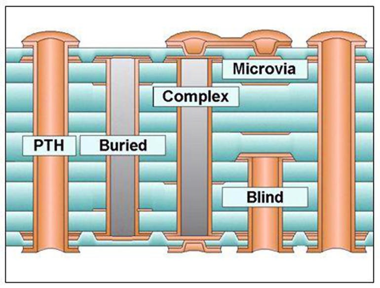
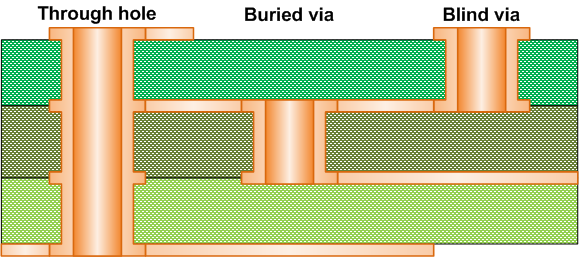
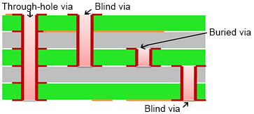
Blind and buried vias are only available on boards with at least four layers. Unlike regular vias on a two layer board which connect the two surface layers, buried and blind vias connect the inner layers with either other adjacent inner layers or adjacent surface layers.

Blind Vias: Connects an inner layer with the adjacent surface layer, they are only visible on one side of the boards and so are called ‘blind’ vias. 

Buried Vias: Connects two adjacent inner copper layers. They are not visible from the surface and so are ‘buried’.

Advantages and disadvantages

Using blind and buried vias in a PCB design has its advantages and disadvantages. The advantage, of course is that this technology offers a viable design technique to help meet the density constraints of lines and pads on a typical design without increasing the layer count or board size. The disadvantage of the technology is that due to the additional operations in manufacturing the board, the cost of a board using blind and/or buried vias is significantly higher than a typical multilayer_ board with the same number of layers.


Peck Drilling Blind Vias

Drill depth is extremely important in vias, because going too shallow or too deep can have a dangerous impact on the board. You can also create spurs and rough edges that cause issues if you’re not being careful.

That said, companies can reduce cost with blind vias if they’re made through peck drilling. Peck drilling plunges the drill into the board multiple times in order to remove material buildup and prevent rough spots.

What Is a Via?

Vias are the copper-plated holes in the printed circuit board that allows the layers to connect. The standard via is called a through-hole via, but there are several disadvantages to using through-hole vias in Surface Mount Technology (SMT). For this reason, we often use a blind via or buried via instead. A blind or buried via can be processed in a wide range of different measures, including plugged copper mask via, a plugged solder mask via, plated via or staggered via.

• What Is a Blind Via?

In a blind via, the via connects the external layer to one or more inner layers of the PCB and is responsible for the interconnection between that top layer and the inner layers.


• What Is a Buried Via?


In a buried via, only the inner layers of the board are connected by the via. It is “buried” inside the board and not visible from the outside.


Blind and buried vias are particularly advantageous in HDI PCBs because they optimize the density of the boards without increasing board size or the number of board layers you require.


• What Is a Stacked Via and Microvia?

A stacked via is a way to further improve size and density considerations when manufacturing printed circuit boards — factors that are extremely important with today’s miniaturization and high-signal transmission speed requirements in many applications.

If you have blind vias with an aspect ratio greater than 1:1, or your drilling needs cover multiple layers, a stacked via can be the best way to get a reliable internal connection.

Stacked vias are laminated blind or buried vias, multiple vias inside a circuit board built together around the same center. Staggered vias are laminated vias that are not around the same center. The advantages of stacked vias include not only saving space and increasing density, but greater flexibility concerning the inner connections, better routing capacity and less parasitic capacitance. The downside of stacked vias is that they come with a higher cost than standard through-hole vias or blind/buried vias.

A microvia is merely a very small via. As you can imagine, microvias are very desirable to PCB designers — the smaller the diameter, the more routing space you have on the board and the lower the parasitic capacitance, which is essential for high-speed circuits. However, very small vias also require more drilling time and more off-center via moves. GoJGo defines microvias as vias with diameters of less than 0.1mm.

Contact GoJGo for PCBs With Blind/Buried Vias and Stacked Vias/Microvias

GoJGo has years of experience manufacturing printed circuit boards using blind and buried vias. No matter what it takes, we can make exactly the blind or buried via PCB you need for your applications. The following table shows design parameters on blind vias and buried vias manufactured by GoJGo:

• Via Type Via Diameter

Via TypeVia Diameter
(max.)
Via Diameter
(min.)
Via PadAnnular RingAspect Ratio
Blind via (mechanical)0.4mm150μm450μm127μm1:1
Blind via (laser)0.1mm100μm254μm150μm1:1
Buried via (mechanical)0.4mm100μm300μm150μm1:10
Buried via (laser)0.4mm100μm225μm150μm1:12

Get in touch with us today to learn more about the various types of vias and how we use them to optimize the value of your printed circuit boards. For a free quote on your printed circuit board project by clicking below button.

Free PCB Request for Quotation (RFQ)

1. You can send email to us (tedchen163@yahoo.com). We will provide you with a
solution to make your PCB cost lower.
2. GoJGo receive your order,review the first,if there are questions,we will communicate with you
the first time and answer you about the lead time.
3. Our Engineering department will review this order with relevant departments,Produced in the best
process and in the shortest time.
4. Before shipment,we will talk with you about the shipping time and shipping method.

If you would like to customize your PCB type and place an order online, please click below to request a quotation.